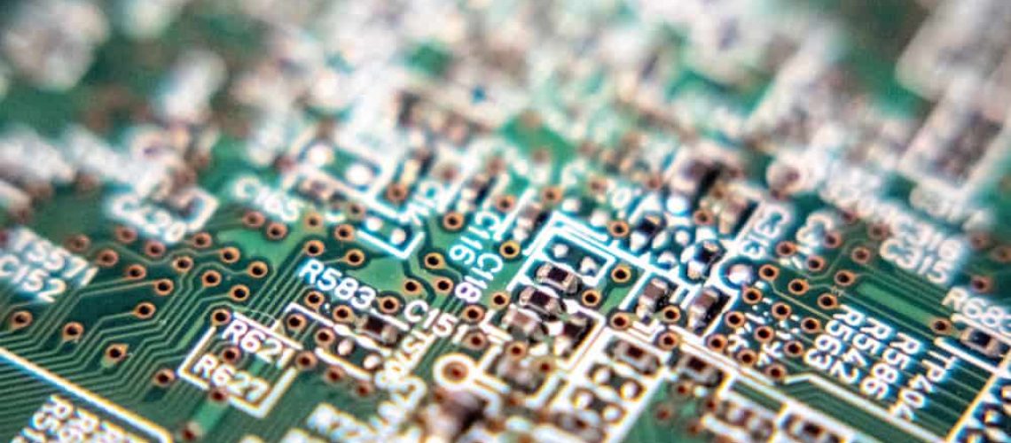
According to a report by GSMA Intelligence, more than 5 billion people globally have access to a mobile device, with over half of these connections being smartphones. Printed circuit boards (PCBs) are at the heart of electronic device manufacturing, including cellphones, TVs, computers, and much more.
How to Assemble Printed Circuit Boards
The circuit board assembly for custom projects is an intricate process that integrates your design plans with PCBA manufacturing expertise. The small green chip covered in lines that you see requires proper preparation and design to provide the expected functionality after the components are fitted in. After design-for-manufacturing checks and inspection, the PCB manufacturer deposits the copper on the board in preparation to fit in the components.
The manufacturer may use one of the two major mounting technologies to assemble printed circuit boards: through-hole technology or surface mount technology. Here is a more detailed look into the two assembly processes.
Surface Mount Technology
The surface mount assembly rose to popularity in the 1980s and has become the standard for modern-day manufacturing of PCBs. The process to assemble printed circuit boards utilizes components with metal tabs that can be easily soldered on the surface, as opposed to inserting them through holes.
The technology allows you to utilize both sides of the electrical board for electrical wiring. The manufacturer will apply solder paste on the board using a PCB stencil or solder screen to ensure correct application. The assembler will then attach the components to the pads found on the surface.
Pros and Cons of SMT
The assembly and manufacture of the circuit boards are quicker and cheaper, allowing for easier scaling of production. Surface-mounted PCBs are ten times lighter and three times smaller than through-hole PCBs. With both sides being available for attachment, it may provide for additional components of high-quality circuit boards. Sadly, SMT produces unreliable circuit boards for equipment that experiences frequent shocks or collisions.
Through-Hole Technology
Through-hole manufacturing is a design standard for circuit board assembly where the PCB components are mounted using pins inserted through pre-drilled holes on one side of the board and soldered to pads on the opposite side. The technology was an instant hit since its inception in the 1940s until the emergence of SMT in the late 1980s.
There are modern electronics that still utilize the technology, including transformers, capacitors, and semiconductors. The PCB assembly involves drilling holes through the circuit board, inserting the components, and soldering them on the other side. The initial process was manual and labor-intensive. Currently, the process utilizes automated insertion machines, which are faster and more precise.
Pros and Cons of Through-Hole Technology
The greatest advantage of through-hole processes is the stronger physical connection of the PCB components. Additionally, the printed circuit boards are more heat-tolerant and can withstand higher environmental stress and impact collisions. Sadly, the manufacturing process entails precise drilling of holes through the circuit board, making it costly and time-consuming. The holes also take up spaces that would fit additional components.
Printed circuit boards are critical parts of any electrical device. The technology used to assemble printed circuit boards may vary depending on your design and application. For more information on the design process for your custom printed circuit boards, reach out to Mathis Electronics.


